0
0

Battery-powered IoT devices, wearables, and consumer electronics face a persistent engineering tension: users expect continuous motion sensing and responsive gesture recognition, yet every milliampere of current draw erodes the battery life that determines product viability. The LSM6DSOTR from STMicroelectronics addresses this challenge directly, combining a 3-axis digital accelerometer and a 3-axis digital gyroscope into a compact system-in-package that operates at 0.55 mA in combo high-performance mode while enabling always-on low-power features for both sensing elements. This balance between capability and efficiency is the defining characteristic of a device that ST describes as delivering “an optimal motion experience for the consumer”.
Housed in a 2.5 mm × 3.0 mm × 0.83 mm LGA-14L package, the LSM6DSOTR represents the modern-generation mainstream offering in ST's iNEMO family. It incorporates MIPI I3C℠ support alongside I²C and SPI, a smart FIFO that compresses up to 9 kbyte, and a 16-program finite state machine capable of executing motion recognition tasks autonomously.
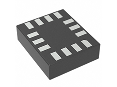
The most consequential specification of the LSM6DSOTR for system designers is its 0.55 mA combo high-performance current consumption. This figure reflects simultaneous operation of both the accelerometer and gyroscope in high-performance mode, not a degraded single-sensor configuration. Equally important, the device offers multiple power modes ranging from low-power to high-performance, allowing firmware to dynamically trade measurement fidelity for current consumption based on operational context-.
The accelerometer can operate at output data rates as low as 1.6 Hz in low-power mode, a setting appropriate for step counting and activity classification where per-sample power dominates total energy consumption. When higher bandwidth is needed, the device scales to 6.66 kHz for both the accelerometer and gyroscope.
The LSM6DSOTR embeds a 16-program finite state machine that processes data from the accelerometer, gyroscope, and external sensors. Each FSM program is intended to detect a specific gesture or motion pattern, operating independently and asserting interrupts when its condition is met-. This architecture allows common motion recognition tasks — such as detecting a wrist raise, recognizing a specific activity transition, or implementing custom gesture controls — to execute entirely within the sensor, eliminating the need for continuous host processor involvement.
The device includes a Smart FIFO with 3 kbyte of native storage that expands to 9 kbyte effective capacity through data compression. This compression operates on motion data streams by exploiting redundancy in consecutive samples, achieving compression ratios of 2× or 3× depending on data variance. For a wearable device sampling at 26 Hz, the compressed FIFO provides several seconds of buffering, enabling the host to wake at intervals rather than on every sample.
Unlike older-generation IMUs that offered only I²C and SPI, the LSM6DSOTR adds MIPI I3C℠ support, a modern interface specification that reduces pin count while maintaining high data rates. The device also features an auxiliary SPI interface for OIS/EIS data output, supporting both optical and electronic image stabilization functions. Independent I/O supply operation at 1.62 V enables direct interface with low-voltage application processors without level shifting.
The following table summarizes the primary technical parameters of the LSM6DSOTR.
|
Parameter |
Specification |
|
Accelerometer Full Scale |
±2 / ±4 / ±8 / ±16 g |
|
Gyroscope Full Scale |
±125 / ±250 / ±500 / ±1000 / ±2000 dps |
|
Output Data Rate |
Up to 6.66 kHz; accel. down to 1.6 Hz in LP |
|
Resolution |
16-bit |
|
FIFO |
3 kbyte native, up to 9 kbyte with compression |
|
Host Interface |
I²C (400 kHz), SPI (10 MHz), MIPI I3C℠ (SDR) |
|
Auxiliary Interface |
SPI for OIS/EIS |
|
Embedded Engine |
16-program finite state machine |
|
Supply Voltage (VDD) |
1.71 V to 3.6 V |
|
Supply Voltage (VDD_IO) |
1.62 V (independent) |
|
Current (Combo HP Mode) |
0.55 mA typ. |
|
Operating Temperature |
−40 °C to +85 °C |
|
Package |
LGA-14L, 2.5 × 3.0 × 0.83 mm |
|
Device ID (WHO_AM_I) |
0x6C |
|
Compliance |
RoHS / REACH, ECOPACK (halogen-free) |
The LSM6DSOTR is best understood not as a passive sensor but as an intelligent motion processing node. Its architecture layers several levels of capability between the physical sensing elements and the host interface.
Sensor Layer. Three-axis accelerometer and three-axis gyroscope sensing elements, fabricated using ST's proven MEMS processes, form the measurement foundation. Both sensors operate independently with separate output data rates and power mode settings, allowing asymmetric configurations optimized for specific use cases.
Signal Processing Layer. 16-bit ADCs digitize the analog sensor outputs, followed by configurable digital filtering. The signal chain for each axis can be tuned to balance noise performance against bandwidth requirements.
Decision Layer. The 16-program FSM executes concurrently, examining sensor data streams and evaluating them against programmed conditions. This enables hardware-level event detection for free-fall, wake-up, 6D/4D orientation, click and double-click, activity/inactivity, and stationary/motion states.
Buffering Layer. The Smart FIFO accumulates data with optional timestamping, supporting both streaming and batch modes. The compression feature allows effective storage capacity to expand based on data characteristics.
Interface Layer. The device supports four connection modes. Mode 1 offers I²C/I3C slave or SPI interface. Mode 2 adds I²C master for external sensor connectivity. Modes 3 and 4 enable the auxiliary SPI interface for OIS applications — Mode 3 for gyroscope data only, Mode 4 for both accelerometer and gyroscope data.
Smartwatches and fitness trackers require continuous motion sensing for step counting, activity classification, sleep staging, and gesture recognition. The LSM6DSOTR's low-power modes allow the accelerometer to run continuously at modest data rates while the gyroscope remains available for gesture detection, all within a power budget compatible with multi-day battery life. ST's advanced pedometer, step detector, and step counter functions are embedded in hardware, reducing host processing overhead.
The LSM6DSOTR has been deployed in low-power IoT systems for applications including respiration monitoring and unauthorized access detection-. In these designs, the sensor's ability to operate in a sleep state and wake on motion events, combined with FIFO data batching, allows the system to achieve extended battery life while maintaining reliable event detection.
Android compliance and support for real, virtual, and batch sensors make the LSM6DSOTR directly compatible with smartphone motion processing frameworks. The MIPI I3C interface aligns with modern mobile platform architectures, while the auxiliary SPI for OIS/EIS supports camera stabilization functions.
The combination of low-latency interrupt response, programmable FSM for gesture recognition, and the auxiliary SPI interface positions the LSM6DSOTR for motion-based gaming controllers and AR/VR input devices. Its compact footprint suits the tight spatial constraints of handheld controllers and head-mounted accessories.
The auxiliary SPI interface provides a dedicated channel for OIS and EIS data at rates suitable for real-time image stabilization. By separating the stabilization data path from the main application processor interface, the LSM6DSOTR enables camera subsystems to maintain stabilization responsiveness independently of other system activities.
The LSM6DSOTR's independent I/O supply capability deserves particular attention during system design. With VDD_IO as low as 1.62 V and VDD ranging from 1.71 V to 3.6 V, the device can interface directly with low-voltage application processors while operating from a higher main supply rail, simplifying power tree design.
The 9 kbyte compressed FIFO transforms system-level power management. Rather than polling the sensor at its configured output data rate, the host can enter a low-power state and be awakened by FIFO threshold interrupts when sufficient data has accumulated. For a typical wearable operating at 52 Hz ODR, the host might wake every 2–3 seconds to drain the FIFO, reducing average system current substantially.
The FSM operates independently of the host processor, allowing motion detection functions to remain active in system states where the application processor is powered down or in deep sleep. This architectural feature enables the “always-on” sensing capability that defines the device's value proposition for battery-constrained designs.
The LSM6DSOTR delivers a carefully balanced combination of low power consumption, embedded intelligence, and interface flexibility. Its 0.55 mA combo high-performance current establishes a practical power ceiling for always-on 6-axis sensing, while the programmable FSM and Smart FIFO offload motion processing tasks from the host processor. The addition of MIPI I3C℠ alongside traditional I²C and SPI ensures compatibility with current and emerging platform architectures. For system designers building battery-powered devices where motion sensing must be continuous, responsive, and power-efficient, the LSM6DSOTR provides the functional density and architectural separation needed to meet those requirements within a 2.5 × 3.0 mm footprint.
WELL LINK CHIPS GROUP CO.,LIMITED FLAT/RM 1802 BEVERLY HOUSE 93-107 LOCKHART ROAD WANCHAI HK