0
0

The HMC424ALP3ETR is a broadband, 6-bit gallium arsenide (GaAs) digital attenuator housed in a compact 3 mm × 3 mm leadless surface-mount package. Covering a frequency range from DC to 13 GHz, this device provides a total attenuation control range of 31.5 dB in precise 0.5 dB steps, making it a versatile building block for RF and microwave signal chain designs where accurate amplitude control is essential.
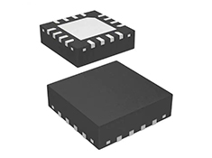
The attenuator employs a 6-bit parallel control architecture that allows users to program the attenuation state via six control voltage inputs toggled between 0 V and VEE. Its monolithic GaAs design integrates the entire attenuation network onto a single die, eliminating the need for discrete component matching and ensuring consistent performance across the operating band.
The HMC424ALP3ETR operates across an exceptionally wide frequency range from 0.1 GHz to 13.0 GHz, spanning portions of the L-band, S-band, C-band, X-band, and Ku-band. This wide coverage enables a single attenuator design to serve multiple frequency plans, reducing component count and simplifying inventory management in multi-band RF systems.
The 6-bit digital control provides attenuation steps of 0.5 dB (LSB), 1 dB, 2 dB, 4 dB, 8 dB, and 16 dB. This binary-weighted bit arrangement delivers a total attenuation of 31.5 dB with a typical step error of only ±0.5 dB, ensuring precise amplitude control across the full range.
The device achieves attenuation accuracy of ±(0.2 dB + 4% of attenuation state), a specification that ensures reliable, repeatable performance in applications requiring precise signal level control. This level of accuracy is critical in test instrumentation and communication systems where amplitude errors directly impact measurement uncertainty and system performance.
With a third-order intercept point (IIP3) of +38 dBm typical and a 0.1 dB compression point of 22 dBm typical, the HMC424ALP3ETR maintains signal integrity even in the presence of strong interfering signals. This linearity performance is essential in receiver front-ends and multi-carrier systems where intermodulation distortion must be minimized.
The attenuator exhibits a typical insertion loss of less than 4 dB across the specified frequency range, with 3.9 dB specified as the insertion loss parameter. This low loss preserves signal-to-noise ratio through the attenuation stage and reduces the need for additional gain compensation in the signal chain.
|
Parameter |
Specification |
|
Frequency Range |
0.1 GHz to 13.0 GHz |
|
Attenuation Range |
31.5 dB |
|
Attenuation Step Size |
0.5 dB (LSB) |
|
Bit Values |
0.5, 1, 2, 4, 8, 16 dB |
|
Insertion Loss |
< 4 dB typ. |
|
Attenuation Accuracy |
±(0.2 dB + 4% of atten. state) |
|
Step Error |
±0.5 dB typ. |
|
Input IP3 |
+38 dBm typ. |
|
Input P1dB |
22 dBm typ. (VEE = -3V) |
|
Supply Voltage (VEE) |
-3 V to -5 V |
|
RF Input Power (Max) |
25 dBm |
|
Control Interface |
6 parallel control lines (0 V / VEE) |
|
Switching Speed |
30 ns rise/fall typ. |
|
Operating Temperature |
-40 °C to +85 °C |
|
Package |
16-lead LFCSP, 3 × 3 mm |
|
MSL Rating |
MSL 3 (168 hours) |
The device operates from a single negative supply voltage ranging from -3 V to -5 V, with the VEE bias allowing operation at frequencies down to DC. An external level shifter is required to interface the control inputs with standard CMOS or TTL logic levels.
The attenuation function is implemented using GaAs MESFET switches arranged in a binary-weighted topology. Each bit of attenuation is controlled by a dedicated switch cell that either passes the signal through or routes it through a calibrated attenuation network. The monolithic construction ensures that the attenuation states are precisely matched and that performance is consistent from unit to unit.
Six parallel control inputs select the attenuation state by toggling between 0 V and VEE. The binary-weighted control allows any attenuation value from 0 dB to 31.5 dB to be selected in 0.5 dB increments by applying the appropriate 6-bit control word. The simple parallel interface requires no serial programming or register configuration, enabling fast switching and straightforward system integration.
The control inputs are referenced to VEE, requiring an external level shifter when interfacing with ground-referenced CMOS or TTL logic. This design choice ensures that the attenuator's RF performance is not compromised by control signal coupling, as the control lines are isolated from the RF ground reference.
The RF input and output ports are internally matched to 50 Ω, eliminating the need for external matching networks. The signal path through the attenuator maintains a consistent characteristic impedance across all attenuation states, minimizing return loss variations during state transitions.
In base station transceiver designs, the HMC424ALP3ETR provides precise gain control in the transmit and receive chains. Its high linearity ensures that strong adjacent-channel signals do not generate intermodulation products that would degrade receiver sensitivity or violate spectral emission requirements-1.
Very small aperture terminal (VSAT) systems and point-to-point microwave radios require accurate amplitude control to maintain link margin under varying atmospheric conditions. The attenuator's wide frequency coverage supports multiple frequency bands within a single platform, while its 0.5 dB resolution enables fine adjustment of transmit power and receive gain.
In automatic test equipment (ATE) and laboratory instrumentation, the HMC424ALP3ETR provides programmable attenuation for signal level calibration and path loss compensation. The 30 ns typical switching speed enables rapid state changes during test sequences, while the ±0.5 dB step accuracy ensures measurement repeatability.
The device's operating temperature range of -40 °C to +85 °C and robust construction support use in military communication, radar, and electronic warfare systems. The wide frequency coverage accommodates the multiple bands typically required in these platforms, and the high linearity ensures reliable operation in dense signal environments.
In fiber optic transceiver modules and broadband telecom equipment, the HMC424ALP3ETR provides level control for RF signals that are converted to or from optical carriers. Its low insertion loss and flat frequency response across the operating band maintain signal fidelity through the attenuation stage.
The HMC424ALP3ETR's 3 mm × 3 mm LFCSP package occupies minimal board area while providing adequate thermal dissipation for its power handling requirements. The exposed pad should be soldered to a grounded thermal land to ensure reliable operation and mechanical stability.
The parallel control interface simplifies digital control design: each attenuation bit requires only a single control line, and no clock or data signals are needed. However, designers must provide level-shifting circuitry between the system's logic supply and the VEE-referenced control inputs. A common approach uses a level shifter IC or discrete transistor-based level translation.
For applications requiring attenuation at frequencies down to DC, a single -5 V VEE supply is recommended, as the device's performance specifications are characterized under this condition. The maximum RF input power of 25 dBm provides substantial headroom for typical signal chain power levels.
The HMC424ALP3ETR delivers broad frequency coverage, fine attenuation resolution, and high linearity in a compact surface-mount package. Its 6-bit parallel control architecture provides straightforward digital programming, while the GaAs MMIC construction ensures consistent performance across the full DC to 13 GHz operating range. For RF and microwave system designers seeking precise amplitude control with minimal insertion loss and excellent repeatability, this digital attenuator offers a well-characterized, production-proven solution.
WELL LINK CHIPS GROUP CO.,LIMITED FLAT/RM 1802 BEVERLY HOUSE 93-107 LOCKHART ROAD WANCHAI HK