0
0

The STM32F405RGT6 is a high-performance microcontroller from STMicroelectronics built on the ARM Cortex-M4 32-bit RISC core with floating-point unit and DSP instructions, operating at up to 168 MHz. It combines 1 Mbyte of Flash memory and 192+4 Kbytes of SRAM with a rich peripheral set in a 64-pin LQFP package, delivering 210 DMIPS of computational performance for demanding embedded applications.
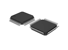
The STM32F405RGT6 belongs to ST's high-performance foundation line, which prioritizes raw processing capability and peripheral integration over the aggressive power optimization found in the L-series. The device's ART Accelerator enables zero-wait-state execution from Flash memory at full clock speed, making it suitable for applications ranging from motor control and industrial automation to audio processing and advanced human-machine interfaces.
The ARM Cortex-M4 core with FPU delivers 210 DMIPS at 168 MHz (1.25 DMIPS/MHz) and implements a full set of DSP instructions. The single-precision floating-point unit accelerates mathematical operations, making the device well-suited for control algorithms, audio processing, and sensor fusion applications that benefit from floating-point arithmetic.
The Adaptive Real-Time (ART) Accelerator allows zero-wait-state execution from Flash memory, eliminating the performance penalty typically associated with executing code from embedded non-volatile memory. This enables the processor to run at full speed without the need for complex cache management or external memory interfaces, simplifying system design while maximizing performance.
With 1 Mbyte of Flash memory and up to 192+4 Kbytes of SRAM including 64 Kbytes of core-coupled memory (CCM) data RAM, the STM32F405RGT6 provides substantial storage for application code, data buffers, and real-time operating system requirements. The CCM RAM is tightly coupled to the core for low-latency access, ideal for time-critical data structures.
Three 12-bit ADCs with 2.4 MSPS conversion rate support up to 24 channels, with 7.2 MSPS achievable in triple interleaved mode. Two 12-bit DACs provide analog output capability. These analog resources enable direct interfacing with sensors, actuators, and analog signal conditioning circuits without external converter components.
Up to 15 communication interfaces are available, including three I²C ports, four USARTs, two UARTs, three SPIs with 42 Mbit/s throughput, two CAN 2.0B interfaces, an SDIO interface, and a USB 2.0 full-speed OTG controller with on-chip PHY. This interface density supports complex system architectures with multiple external devices and network connectivity.
The FSMC supports external memory expansion with CompactFlash, SRAM, PSRAM, NOR, and NAND interfaces. An LCD parallel interface with 8080/6800 modes enables direct connection to display modules, making the device suitable for graphical user interface applications.
|
Parameter |
Specification |
|
Core |
ARM Cortex-M4 with FPU and DSP |
|
Max Frequency |
168 MHz |
|
DMIPS |
210 (1.25 DMIPS/MHz) |
|
Flash Memory |
1 Mbyte |
|
SRAM |
192+4 Kbytes (64 KB CCM) |
|
Operating Voltage |
1.8 V to 3.6 V |
|
Temperature Range |
-40 °C to 85 °C |
|
ADC |
3 × 12-bit, 2.4 MSPS (7.2 MSPS interleaved) |
|
DAC |
2 × 12-bit |
|
Timers |
17 total (12 × 16-bit, 2 × 32-bit) |
|
Communication |
I²C, SPI, USART, UART, CAN, USB OTG, SDIO |
|
External Memory |
FSMC for CF, SRAM, PSRAM, NOR, NAND |
|
Display Interface |
LCD parallel, 8080/6800 modes |
|
I/O Pins |
51 (up to 140 on larger packages) |
|
Package |
LQFP64, 10 × 10 × 1.4 mm |
|
Grade |
Industrial |
The device operates from a supply voltage of 1.8 V to 3.6 V, providing compatibility with a wide range of system power architectures. The 210 DMIPS processing capability and integrated floating-point unit enable execution of complex algorithms in real time, while the comprehensive peripheral set reduces the need for external companion chips.
The Cortex-M4 core implements the ARMv7E-M architecture with hardware floating-point support (single precision) and DSP extensions. The memory protection unit (MPU) enhances application security by defining access permissions for different memory regions. The multi-AHB bus matrix enables parallel access between the core, DMA controllers, and peripherals, maximizing system throughput.
The clock system supports multiple sources including a 4-to-26 MHz crystal oscillator, an internal 16 MHz factory-trimmed RC oscillator with 1% accuracy, and a 32 kHz oscillator for the real-time clock. Three PLLs provide flexible clock multiplication for the system clock, audio peripherals, and ADC. Power-on reset (POR), power-down reset (PDR), programmable voltage detector (PVD), and brown-out reset (BOR) ensure reliable startup and operation under varying supply conditions.
The three ADCs can be configured for independent or interleaved operation, with the latter achieving 7.2 MSPS aggregate sampling rate. The DACs include output buffers and can generate waveforms for audio or control applications. The integrated temperature sensor provides on-chip thermal monitoring.
The USB OTG controller supports full-speed device, host, and OTG modes with an on-chip PHY, eliminating the need for external transceivers. The two CAN interfaces support 2.0B Active protocol for automotive and industrial network connectivity. The SDIO interface enables direct connection to SD memory cards and SDIO peripherals. The SPI interfaces support 42 Mbit/s throughput with muxed full-duplex I²S capability for audio applications.
The STM32F405RGT6's advanced timers, including two PWM timers for motor control with quadrature encoder inputs, make it well-suited for field-oriented control of brushless DC and permanent magnet synchronous motors. The DSP instructions and FPU accelerate the mathematical transformations required by motor control algorithms.
The combination of the FPU, DSP instructions, and I²S interfaces with audio-class accuracy enables real-time audio processing applications including effects processors, digital mixers, and audio codecs. The 168 MHz core provides sufficient computational headroom for complex filtering and mixing algorithms.
The LCD parallel interface and FSMC support direct connection to graphical displays, while the processing power enables smooth rendering of user interfaces. The device's memory resources accommodate graphical frame buffers and touchscreen processing without external memory.
The high-resolution ADCs and DACs, combined with the processing performance, support medical instrumentation applications such as patient monitors, diagnostic equipment, and laboratory instruments. The USB OTG interface enables data transfer to host computers or storage devices.
Applications ranging from robotics and drones to industrial control and test equipment benefit from the STM32F405RGT6's combination of processing power, memory resources, and peripheral integration. The device provides a platform that can handle complex control algorithms, multiple communication protocols, and real-time operating system requirements simultaneously.
The STM32F405RGT6's 64-pin LQFP package provides 51 I/O pins, with most being 5 V-tolerant for compatibility with legacy peripherals and industrial interfaces. The pinout is designed for efficient PCB routing, with power and ground pins distributed to minimize noise coupling.
The FSMC and LCD parallel interface consume a significant number of I/O pins. Designers planning to use these features should carefully evaluate pin allocation against other peripheral requirements. The CCM RAM provides a low-latency memory region that can be used for stack, heap, or time-critical data structures, separate from the main SRAM accessible by DMA controllers.
For applications requiring the highest ADC performance, care must be taken in PCB layout to isolate analog supply and ground from digital noise sources. The device includes separate analog supply pins to facilitate this isolation.
The STM32F405RGT6 delivers high-performance computing with the ARM Cortex-M4 core, floating-point unit, and DSP instructions, supported by generous memory resources and a comprehensive peripheral set. Its 168 MHz operating frequency and 210 DMIPS processing capability enable execution of demanding real-time algorithms, while the ART Accelerator ensures that this performance is achieved without wait states from Flash memory. With three ADCs, two DACs, USB OTG, CAN, and a flexible static memory controller, the device provides the integration needed to reduce system complexity and cost. For embedded applications where processing performance is the primary design driver, the STM32F405RGT6 offers a well-balanced, production-proven platform.
WELL LINK CHIPS GROUP CO.,LIMITED FLAT/RM 1802 BEVERLY HOUSE 93-107 LOCKHART ROAD WANCHAI HK