0
0

The SKY66394-11 from Skyworks Solutions is a fully input/output matched power amplifier (PA) designed for FDD and TDD 2G/3G/4G LTE small cell base stations operating in the 2000 to 2300 MHz frequency band. This highly integrated device delivers 38 dB of gain with 35% power-added efficiency at +28 dBm linear output power, housed in a compact 5 × 5 × 1.3 mm multi-chip module (MCM) package.
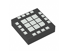
What distinguishes the SKY66394-11 is its combination of high linearity and high efficiency in a fully matched, single-supply design. The integrated active bias circuitry compensates performance over temperature, voltage, and process variation, eliminating the need for external bias networks and simplifying thermal management in dense small cell deployments. As part of a pin-to-pin compatible PA family supporting all 3GPP bands, the device enables platform designs that can be scaled across frequency bands with minimal layout changes.
The SKY66394-11 achieves 35% power-added efficiency (PAE) at +28 dBm linear output power, a level of efficiency that significantly reduces power consumption and heat dissipation in small cell base stations. In dense deployments where multiple PAs operate simultaneously, this efficiency translates directly into lower operating costs and reduced thermal management complexity.
The device delivers +28 dBm linear output power with adjacent channel leakage ratio (ACLR) better than -50 dBc when used with digital pre-distortion (DPD) for a 40 MHz LTE signal with 8.5 dB peak-to-average power ratio. This linearity performance ensures compliance with 3GPP spectral emission requirements while maintaining efficient operation.
With 38 dB typical gain at the test frequency of 2.14 GHz, the SKY66394-11 provides substantial signal amplification in a single stage, reducing the number of gain stages required in the transmit chain. The high gain also simplifies the output power requirements for the preceding driver amplifier.
The PA is internally matched to 50 Ω at both input and output, eliminating the need for external matching networks. This feature reduces bill-of-materials count, minimizes board area, and eliminates the performance variability associated with discrete matching component tolerances.
The on-chip active bias circuitry compensates PA performance over temperature, voltage, and process variation without requiring external bias resistors or thermistors. This integration ensures consistent performance across the operating temperature range of -40 °C to +85 °C and simplifies system-level thermal design.
A dedicated enable pin (PAEN) with a control voltage range of 1.7 V to 2.5 V allows the PA to be turned on and off under logic control. This feature supports TDD operation and enables power-saving modes during periods of low traffic.
|
Parameter |
Specification |
|
Frequency Range |
2000 to 2300 MHz |
|
Test Frequency |
2.14 GHz |
|
Gain |
38 dB typ. |
|
OIP3 |
35.3 dBm typ. |
|
Saturated Power |
35.5 to 36.3 dBm |
|
Linear Output Power |
+28 dBm |
|
PAE @ +28 dBm |
35% |
|
ACLR (with DPD) |
< -50 dBc |
|
Supply Voltage |
5.0 V (4.75 to 5.25 V) |
|
Quiescent Current |
105 mA typ. |
|
Power Dissipation |
1.9 W |
|
Input Return Loss |
12 to 16 dB |
|
Output Return Loss |
10 to 14 dB |
|
Reverse Isolation |
50 dB |
|
Operating Temperature |
-40 °C to +85 °C |
|
Storage Temperature |
-55 °C to +125 °C |
|
Package |
16-pin MCM, 5 × 5 × 1.3 mm |
|
MSL Rating |
MSL3, 260 °C per JEDEC J-STD-020 |
The device operates from a single 5.0 V supply with a quiescent current of 105 mA typical. The power dissipation of 1.9 W requires careful thermal design, but the compact package and high efficiency help minimize the thermal load compared to less efficient PA solutions.
The SKY66394-11 employs a multi-stage amplification topology optimized for high gain and linearity. The input stage provides low-noise amplification, while subsequent stages deliver the power gain required to reach the +28 dBm linear output level. The internal matching networks are designed to present optimal impedances to each amplification stage across the 2000 to 2300 MHz operating band.
The integrated active bias circuit continuously monitors operating conditions and adjusts the bias point to maintain consistent performance over temperature and supply voltage variations. This closed-loop biasing approach eliminates the performance drift that would occur with fixed bias in open-loop designs, ensuring reliable operation across the full -40 °C to +85 °C temperature range.
The PAEN pin provides logic-level control of the amplifier's operating state. When asserted, the device transitions to active mode; when de-asserted, the PA enters a low-power state suitable for TDD switching or power-saving operation. The control voltage range of 1.7 V to 2.5 V is compatible with standard logic levels.
The output matching network is designed to present the optimal load impedance for linear operation while suppressing harmonic content. Second harmonics are specified at -25 to -29 dBc and third harmonics at -55 to -63 dBc, contributing to compliance with 3GPP spurious emission requirements.
The primary application for the SKY66394-11 is in small cell base stations for 2G, 3G, and 4G LTE networks. Small cells are deployed to increase network capacity and coverage in dense urban environments, indoor spaces, and venues. The PA's high efficiency directly addresses the power and thermal constraints of these compact, often pole- or wall-mounted installations.
The device supports 3GPP bands 1, 4, 10, and 23, which cover various frequency allocations worldwide for LTE deployment. The pin-to-pin compatible PA family allows network equipment manufacturers to design a common platform that can be configured for different bands by simply substituting the appropriate PA variant.
In active antenna systems and massive MIMO deployments, the SKY66394-11 provides the per-element amplification required for beamforming and spatial multiplexing. Its compact 5 × 5 mm footprint enables dense integration of multiple PA channels on a single antenna panel, while the high efficiency minimizes the aggregate thermal load of the array.
Beyond small cell applications, the SKY66394-11 can serve as a driver amplifier for macro base station power amplifiers, providing the gain and linearity needed to drive high-power final stages. Its 38 dB gain reduces the output power requirement for the preceding stage, potentially simplifying the transmit chain architecture.
The PA's high linearity and stable performance over temperature also suit point-to-point microwave link applications, where reliable amplification of complex modulated signals is required.
The SKY66394-11's fully matched design simplifies RF board layout: the input and output ports present 50 Ω impedance directly, eliminating the need for matching networks that would otherwise consume board area and introduce loss. The integrated active bias further reduces external component count, as no bias resistors or temperature compensation networks are required.
Thermal design deserves attention given the 1.9 W power dissipation. The 5 × 5 mm package should be soldered to a thermal pad with adequate copper area and thermal vias to conduct heat to the PCB's ground plane. The exposed pad also provides a low-inductance ground connection essential for stable RF performance.
The single 5.0 V supply simplifies power management, but the supply should be well-regulated and adequately decoupled to prevent noise from degrading the PA's linearity. For TDD applications, the PAEN pin allows rapid on/off switching, though the switching transients should be evaluated to ensure they do not violate spectral emission requirements during the transition.
The SKY66394-11 delivers a compelling combination of high gain, excellent linearity, and high efficiency for small cell base station applications in the 2.0 to 2.3 GHz band. Its fully matched, single-supply design simplifies integration while the integrated active bias ensures consistent performance across temperature and supply variations. For network equipment manufacturers seeking a compact, efficient PA solution for 4G LTE and emerging 5G small cell deployments, the SKY66394-11 provides a production-ready building block that balances performance, efficiency, and design simplicity.
WELL LINK CHIPS GROUP CO.,LIMITED FLAT/RM 1802 BEVERLY HOUSE 93-107 LOCKHART ROAD WANCHAI HK