0
0

The TMS320F28335PGFA is a member of Texas Instruments' C2000™ family of 32-bit microcontrollers, purpose-built for real-time control applications that demand a combination of high computational throughput, precise analog-to-digital conversion, and flexible pulse-width modulation generation. Powered by the TMS320C28x core running at up to 150 MHz, this device delivers 150 MIPS of processing capability and integrates an IEEE 754 single-precision floating-point unit (FPU), eliminating the need for software emulation of floating-point arithmetic in control algorithms.
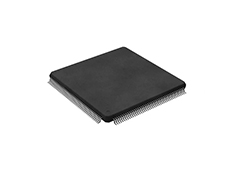
Housed in a 176-pin low-profile quad flatpack (LQFP) package, the TMS320F28335PGFA operates over an industrial temperature range of −40 °C to +85 °C and is rated for catalog-grade applications. Its on-chip memory resources include 256K × 16 words of flash memory and 34K × 16 words of single-access RAM (SARAM), providing ample storage for complex control firmware and data buffers without external memory components.
The TMS320C28x CPU core is a 32-bit fixed-point processor enhanced with an IEEE 754 single-precision floating-point unit, a combination that enables direct execution of floating-point control algorithms without the overhead of software libraries. The core supports 16 × 16 and 32 × 32 multiply-accumulate (MAC) operations and dual 16 × 16 MAC, delivering the arithmetic throughput required for motor control, digital power conversion, and sensorless field-oriented control algorithms.
A dedicated six-channel direct memory access (DMA) controller manages data transfers between the ADC, McBSP, ePWM, XINTF, and SARAM peripherals without CPU intervention. This architectural feature frees the core to focus on control loop execution while sensor data is moved efficiently through the system.
The 16-bit or 32-bit external interface (XINTF) provides access to more than 2M × 16 words of addressable external memory, supporting expansion with SRAM, flash, or other parallel memory devices. This capability is valuable in applications requiring large data buffers or program storage beyond the on-chip resources.
The device includes up to 18 PWM outputs, with up to 6 of them supporting high-resolution PWM (HRPWM) with 150-ps micro-edge positioner (MEP) resolution. Up to 6 event capture inputs and 2 quadrature encoder interfaces (eQEP) are available for position and speed feedback in motor control systems. The device also provides up to 8 32-bit timers and 9 16-bit timers for general-purpose timing functions.
Up to 2 CAN modules, 3 SCI (UART) modules, 2 McBSP modules (configurable as SPI), 1 dedicated SPI module, and 1 I²C bus provide extensive options for inter-system communication and peripheral expansion. This interface density supports the integration of the TMS320F28335PGFA into complex system architectures with multiple external devices.
The on-chip 12-bit ADC features 16 channels with an 80-ns conversion rate, two sample-and-hold units for simultaneous sampling, and a 2 × 8 channel input multiplexer. The ADC supports both single and simultaneous conversion modes, with internal or external reference selection.
|
Parameter |
Specification |
|
Core |
TMS320C28x 32-bit CPU with FPU |
|
Max Frequency |
150 MHz (6.67-ns cycle time) |
|
Processing Performance |
150 MIPS |
|
Core Voltage |
1.9 V / 1.8 V |
|
I/O Voltage |
3.3 V |
|
Flash Memory |
256K × 16 words |
|
SARAM |
34K × 16 words |
|
OTP ROM |
1K × 16 words |
|
Boot ROM |
8K × 16 words |
|
ADC |
12-bit, 16 channels, 80-ns conversion |
|
PWM Outputs |
Up to 18 |
|
HRPWM Outputs |
Up to 6 (150-ps MEP resolution) |
|
Event Capture Inputs |
Up to 6 |
|
Quadrature Encoder Interfaces |
Up to 2 |
|
DMA Channels |
6 |
|
External Interface |
16-bit or 32-bit XINTF |
|
Serial Ports |
2 CAN, 3 SCI, 2 McBSP, 1 SPI, 1 I²C |
|
GPIO Pins |
Up to 88 |
|
Operating Temperature |
−40 °C to +85 °C |
|
Package |
176-pin LQFP (PGF) |
|
Security |
128-bit security key/lock |
The device operates from a 1.9-V/1.8-V core supply and a 3.3-V I/O supply, a voltage architecture that balances performance with compatibility with standard 3.3-V logic interfaces. The 128-bit security key/lock protects flash, OTP, and RAM blocks against unauthorized access and firmware reverse-engineering.
The TMS320C28x core employs a Harvard bus architecture, allowing simultaneous instruction fetch and data access for improved throughput. The unified memory programming model simplifies software development by treating program and data memory as a single address space-3. The peripheral interrupt expansion (PIE) block supports all 58 peripheral interrupts, enabling flexible interrupt prioritization and management.
An on-chip oscillator and watchdog timer module provide the clock generation and system monitoring functions required for reliable embedded operation. The device supports IDLE, STANDBY, and HALT low-power modes, along with the ability to disable individual peripheral clocks for power savings during periods of reduced activity.
Each ePWM module supports independent and complementary PWM generation with adjustable dead-band generation for leading and trailing edges, and a latched or cycle-by-cycle trip mechanism for fault protection-. The HRPWM channels extend the effective resolution of the PWM signal, enabling finer duty cycle control for high-frequency switching applications.
The ADC block contains two sample-and-hold units that permit simultaneous sampling of two channels, a critical capability in motor control applications where phase currents must be measured at the same instant-. The 2 × 8 channel multiplexer allows the converter to service multiple analog inputs sequentially or in interleaved fashion.
The McBSP modules are configurable as SPI interfaces, providing flexibility in protocol selection-3. The CAN modules support the CAN 2.0B protocol for automotive and industrial network connectivity. The boot ROM includes software boot modes through SCI, SPI, CAN, I²C, McBSP, XINTF, and parallel I/O, enabling flexible system startup configurations.
The TMS320F28335PGFA is widely employed as the core processor in motor control applications spanning permanent magnet synchronous motors (PMSM), brushless DC motors (BLDC), and induction motors. Its floating-point unit accelerates the mathematical transformations required by field-oriented control (FOC) algorithms, while the eQEP interfaces provide direct connection to incremental encoders for rotor position feedback. Research demonstrates that the device can execute conventional model predictive current control algorithms in as little as 29 µs, making it suitable for high-performance drive applications-.
In digital power supplies, solar inverters, and active front-end rectifiers, the TMS320F28335PGFA manages the precise timing and control loops that regulate voltage and current. The HRPWM outputs enable fine duty-cycle resolution for high-frequency switching converters, while the 12-bit ADC captures feedback signals for closed-loop control-. The device has been used to implement voltage-oriented control for three-phase active-front-end rectifiers and serial resonant converter controllers-.
The device is used in grid-connected power converters, microgrid inverter control, and renewable energy applications. Its combination of floating-point processing, high-resolution PWM, and comprehensive communication interfaces supports the complex control algorithms required for grid synchronization, power quality improvement, and maximum power point tracking-.
In industrial automation, the TMS320F28335PGFA serves as a motion controller for servo drives, robotic actuators, and multi-axis positioning systems. The CAN interfaces enable integration into industrial networks, while the DMA controller manages sensor data acquisition without interrupting the control loop. Applications include actuator controllers with frequency feedforward parameter compensation and brushless DC motor valve actuators for rapid maneuvering thrusters--.
Beyond control applications, the device is used in data acquisition and real-time signal processing systems. Its 12-bit ADC with simultaneous sampling capability and the floating-point unit's computational power enable implementation of digital filtering, spectral analysis, and real-time monitoring functions in instrumentation and test equipment-.
The TMS320F28335PGFA's 176-pin LQFP package provides up to 88 individually programmable, multiplexed GPIO pins with input filtering, offering substantial flexibility in system I/O allocation. The JTAG boundary scan support, compliant with IEEE Standard 1149.1-1990, facilitates board-level testing and debugging during production and field service.
Development support for the device includes the Code Composer Studio™ integrated development environment, ANSI C/C++ compiler, assembler and linker, and DSP/BIOS™ and SYS/BIOS real-time operating systems. Digital motor control and digital power software libraries are available to accelerate application development, providing pre-validated algorithm building blocks for common control functions.
The device's boot ROM supports multiple boot modes through SCI, SPI, CAN, I²C, McBSP, XINTF, and parallel I/O, allowing system designers to select the most appropriate startup configuration for their application without external configuration hardware. A 128-bit security key/lock mechanism protects the flash, OTP, and RAM contents against unauthorized readout, an important consideration in commercial and industrial products where firmware intellectual property protection is required.
The TMS320F28335PGFA represents a mature, production-proven digital signal controller that combines the computational power of the C28x core with a floating-point unit, a comprehensive set of control-oriented peripherals, and a rich complement of communication interfaces. Its 150 MHz operating frequency, 256K words of flash memory, and 34K words of SARAM provide the processing headroom and memory resources needed for complex real-time control algorithms in motor drives, digital power systems, and industrial automation equipment. The integration of high-resolution PWM outputs, a 12-bit ADC with simultaneous sampling, and quadrature encoder interfaces makes it particularly well-suited for closed-loop motion and power control applications where precise timing and accurate feedback are essential. For designers seeking a well-supported, widely-adopted platform for real-time embedded control, the TMS320F28335PGFA offers a balanced combination of performance, peripheral integration, and development ecosystem maturity.
WELL LINK CHIPS GROUP CO.,LIMITED FLAT/RM 1802 BEVERLY HOUSE 93-107 LOCKHART ROAD WANCHAI HK