0
TPS2320IDR Texas Instruments PMIC - Hot Swap Controllers image
  • TPS2320IDR Texas Instruments PMIC - Hot Swap Controllers image
Images are for reference only

Texas Instruments TPS2320IDR

Manufacturer
Texas Instruments
Mfr. Part #
TPS2320IDR
WLX Part #
A224260008078
Package
16-SOIC (0.154, 3.90mm Width)
Datasheet
TPS2320IDR Datasheet (PDF)

Recommended For You

TPS2320IDR Parameter Description

The TPS2320 and TPS2321 are dual-channel hot-swap controllers that use external N-channel MOSFETs as high-side switches in power applications. Features of these devices, such as overcurrent protection (OCP), inrush-current control, and the ability to discriminate between load transients and faults, are critical requirements for hot-swap applications.

The TPS2320/21 devices incorporate undervoltage lockout (UVLO) to ensure the device is off at startup. Each internal charge pump, capable of driving multiple MOSFETs, provides enough gate-drive voltage to fully enhance the N-channel MOSFETs. The charge pumps control both the rise times and fall times (dv/dt) of the MOSFETs, reducing power transients during power up/down. The circuit-breaker functionality combines the ability to sense overcurrent conditions with a timer function; this allows designs such as DSPs, that may have high peak currents during power-state transitions, to disregard transients for a programmable period.

DISCH1, DISCH2 – DISCH1 and DISCH2 should be connected to the sources of the external N-channel MOSFET transistors connected to GATE1 and GATE2, respectively. These pins discharge the loads when the MOSFET transistors are disabled. They also serve as reference-voltage connections for internal gate voltage-clamp circuitry.

ENABLE or ENABLE – ENABLE for TPS2320 is active low. ENABLE for TPS2321 is active high. When the controller is enabled, both GATE1 and GATE2 voltages will power up to turn on the external MOSFETs. When the ENABLE pin is pulled high for TPS2320 or the ENABLE pin is pulled low for TPS2321 for more than 50 µs, the gate of the MOSFET is discharged at a controlled rate by a current source, and a transistor is enabled to discharge the output bulk capacitance. In addition, the device turns on the internal regulator PREREG (see VREG) when enabled and shuts down PREREG when disabled so that total supply current is much less than 5µA.

FAULT – FAULT is an open-drain overcurrent flag output. When an overcurrent condition in either channel is sustained long enough to charge TIMER to 0.5 V, the overcurrent channel latches off and pulls FAULT low. The other channel will run normally if not in overcurrent. In order to turn the channel back on, either the enable pin has to be toggled or the input power has to be cycled.

GATE1, GATE2 – GATE1 and GATE2 connect to the gates of external N-channel MOSFET transistors. When the device is enabled, internal charge-pump circuitry pulls these pins up by sourcing approximately 15µA to each. The turnon slew rates depend upon the capacitance present at the GATE1 and GATE2 terminals. If desired, the turnon slew rates can be further reduced by connecting capacitors between these pins and ground. These capacitors also reduce inrush current and protect the device from false overcurrent triggering during power up. The charge-pump circuitry will generate gate-to-source voltages of 9 V-12 V across the external MOSFET transistors.

IN1, IN2 – IN1 and IN2 should be connected to the power sources driving the external N-channel MOSFET transistors connected to GATE1 and GATE2, respectively. The TPS2320/TPS2321 draws its operating current from IN1, and both channels will remain disabled until the IN1 power supply has been established. The IN1 channel has been constructed to support 3-V, 5-V, or 12-V operation, while the IN2 channel has been constructed to support 3-V or 5-V operation

ISENSE1, ISENSE2, ISET1, ISET2 – ISENSE1 and ISENSE2, in combination with ISET1 and ISET2, implement overcurrent sensing for GATE1 and GATE2. ISET1 and ISET2 set the magnitude of the current that generates an overcurrent fault, through external resistors connected to ISET1 and ISET2. An internal current source draws 50 µA from ISET1 and ISET2. With a sense resistor from IN1 to ISENSE1 or from IN2 to ISENSE2, which is also connected to the drains of external MOSFETs, the voltage on the sense resistor reflects the load current. An overcurrent condition is assumed to exist if ISENSE1 is pulled below ISET1 or if ISENSE2 is pulled below ISET2. To ensure proper circuit breaker operation, VI(ISENSE1) and VI(ISET1) should never exceed VI(IN1). Similarly, VI(ISENSE2) and VI(ISET2) should never exceed VI(IN2).

TIMER – A capacitor on TIMER sets the time during which the power switch can be in overcurrent before turning off. When the overcurrent protection circuits sense an excessive current, a current source is enabled which charges the capacitor on TIMER. Once the voltage on TIMER reaches approximately 0.5 V, the circuit-breaker latch is set and the power switch is latched off. Power must be recycled or the ENABLE pin must be toggled to restart the controller. In high-power or high-temperature applications, a minimum 50-pF capacitor is strongly recommended from TIMER to ground, to prevent any false triggering.

VREG – VREG is the output of an internal low-dropout voltage regulator, where IN1 is the input. The regulator is used to generate a regulated voltage source, less than 5.5 V, for the device. A 0.1-μF ceramic capacitor should be connected between VREG and ground to aid in noise rejection. In this configuration, upon disabling the device, the internal low-dropout regulator will also be disabled, which removes power from the internal circuitry and allows the device to be placed in low-quiescent-current mode. In applications where IN1 is less than5.5 V, VREG and IN1 may be connected together. However, under these conditions, disabling the device will not place the device in low-quiescent-current mode, because the internal low-dropout voltage regulator is being bypassed, thereby keeping internal circuitry operational. If VREG and IN1 are connected together, a 0.1-µF ceramic capacitor between VREG and ground is not needed if IN1 already has a bypass capacitor of 1µF to 10µF.


Purchase Guide

1. Send Enquiry
You can send an inquiry by email, or add the item to the RFQ list and submit it to us.
Tell us the model and quantity you need, our sales staff will reply the price in time.

sales@welllinkchips.com


2. Receive a quote
You will receive an email with the price, quantity and delivery date of the product you need

3. Payment
You can pay the orders by wire transfer offline. We support: Paypal,VISA.
Please fill the shipping address and express information when placing your order. We support: UPS,DHL,Fedex,SF


Shipping & Delivering

1. Shipping & Delivering
After receiving your payment, we will ship the goods for you within the delivery period and send the shipping number by email

2. Shipping cost already shown on the quote, please check your email.

3.We will evaluate the shipping cost according to the price of the product you purchased and the shipping address. If you need to specify the shipping method, you can notify us by email.

4. We support DHL, FedEx, UPS, SF to ship your goods by default


5.Regarding in stock parts, orders can generally be ready to ship within 4 hours.
We ship daily at 5pm.(UTC/GMT+8)
Once the goods are shipped, estimated delivery time depends on the shipping methods you chose:
FedEx International, 5-7 business days.
DHL Express, 5-7 business days.

The following are some common countries' logistic time.


Note: 

The above table is for reference only, there may will have some delay for the uncontrollable factors.


Refund & Return
Refund
Refunds are normally accepted within 30 days from the date of the parcel delivered. Please contact our support team for any issues immediately once you receive your parcels includes but is not limited to below reasons:
Not received the parcel normally
Yes, we guarantee a refund or to resend your order if you haven't received the parcel beyond the regular shipping days, except the case which customer takes the responsibility for the unsuccessful delivery such as providing an incorrect shipping address, can not complete the customs clearance due to customer's reason, etc. Note: If the following issues occurs: extreme weather, post office delay, customs clearance, local protest, etc. In this case, we are incapable of guaranteeing on-time delivery, but we'll try our best to support you,thanks.
Some items missing from my shipment
First, check that you've received all the boxes associated with your order. Then fully empty each box you received, sometimes small parts get caught in crevices or in packing material. If you still can't find your item, please email customer service right away. Include a description of the missing quantities and pictures of the whole parcel. We'll forward them to our warehouse to check the monitor records and the packing pictures records. Steps:
1. Send email to support team for authorization.
2. We'll check and verify the issues.
3. Offer solutions to customer case by case.
Return
By returning products to WELL LINK CHIPS, the Customer certifies that the products were purchased from WELL LINK CHIPS and there has been no substitution in whole or part of the same product from another supplier, distributor or other such sources of the product. The return should be in the original packaging and in unused condition (except defective). ESD or moisture-sensitive products should not be opened except under controlled conditions. General Rules: Returns are normally accepted within 365 days from the date of the parcel delivered. When a customer requests a return due to 'non-original/fake/quality problems', a valid quality report from a third-party authoritative organization recognized by our company is required for the return and exchange. Any charges from customs and other fees should be paid by customers if the return reason is customers' reason, such as buy parts mistakenly,etc. Return Freight charges must be prepaid; we will not accept COD shipments.
  • *
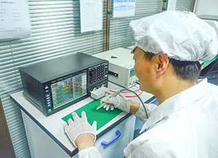
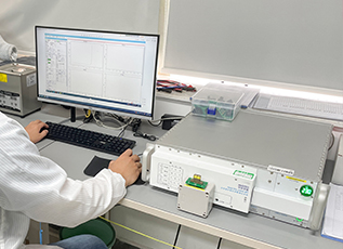
Welllink Chips’ quality control process is carried out in strict accordance with the ISO9001 international quality management system, and quality risks are controlled and reduced through strict supplier control measures + quality testing and other measures.
Supplier level control (Qualified suppliers, provisional suppliers and blacklisted suppliers)
Graded
management
Regular
assessment
Dynamic
management
  • Qualified suppliers
  • Original manufacturers, authorised agents, suppliers without quality incidents.
  • Provisional suppliers
  • Upgrade only if suppliers have passed the profile audit and have worked together 3 times or more without quality incidents.
  • Blacklisted suppliers
  • There is the sale of counterfeit and refurbished parts and the defaulting supplier will be permanently blacklisted.
Quality testing (QC process according to international standards to guarantee product quality)
Testing process:
Primary testing
Labels and outer packaging
Secondary testing
Appearance and electrical properties
Tertiary testing
Slicing, open cap, solderability, ambient temperature, ageing, X-RAY, ultrasound
  • External Visual Inspection

  • Electrical performance testing

  • Key functional testing

  • Key functional testing

  • Slice testing

  • X-RAY Inspection

Stock: Contact to confirm inventory

Please send RFQ , we will respond immediately.

Submit a request