
 0
0
 AD7091R-2BCPZ-RL7 Datasheet (PDF)
24-TSSOP (0.173", 4.40mm Width)
10-WFDFN Exposed Pad, CSP
16-TSSOP (0.173", 4.40mm Width)
20-TSSOP (0.173", 4.40mm Width)
8-UFDFN Exposed Pad, CSP
8-UFDFN Exposed Pad, CSP
20-WFQFN Exposed Pad, CSP
10-TFSOP, 10-MSOP (0.118", 3.00mm Width)
20-WFQFN Exposed Pad, CSP
20-WFQFN Exposed Pad, CSP
10-TFSOP, 10-MSOP (0.118", 3.00mm Width)
16-TSSOP (0.173", 4.40mm Width)

The AD7091R-2 / AD7091R-4 / AD7091R-8 family is a multichannel 12-bit, ultralow power, successive approximation analog-to-digital converter (ADC) that is available in two, four, or eight analog input channel options. The AD7091R-2 / AD7091R-4 / AD7091R-8 operate from a single 2.7 V to 5.25 V power supply and are capable of achieving a sampling rate of 1 MSPS.
The AD7091R-2 / AD7091R-4 / AD7091R-8 family offers up to eight single-ended analog input channels with a channel sequencer that allows a preprogrammed selection of channels to be converted sequentially. The AD7091R-2 / AD7091R-4 / AD7091R-8 also feature an on-chip conversion clock, an on-chip accurate 2.5 V reference, and a high speed serial interface.
The AD7091R-2 / AD7091R-4 / AD7091R-8 have a serial port interface (SPI) that allows data to be read after the conversion while achieving a 1 MSPS throughput rate. The conversion process and data acquisition are controlled using the CONVST pin.
The AD7091R-2 / AD7091R-4 / AD7091R-8 use advanced design techniques to achieve ultralow power dissipation at high throughput rates. They also feature flexible power management options. An on-chip configuration register allows the user to set up different operating conditions. These include power management, alert functionality, busy indication, channel sequencing, and general-purpose output pins. The MUXOUT and ADCIN pins allow signal conditioning of the multiplexer output prior to acquisition by the ADC.
Applications

sales@welllinkchips.com


The above table is for reference only, there may will have some delay for the uncontrollable factors.




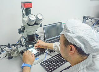
External Visual Inspection
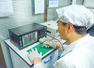
Electrical performance testing
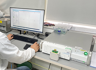
Key functional testing
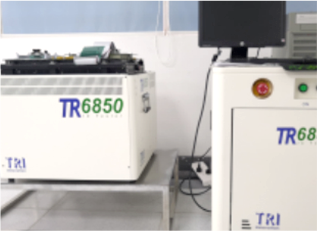
Key functional testing
Slice testing

X-RAY Inspection
WELL LINK CHIPS GROUP CO.,LIMITED FLAT/RM 1802 BEVERLY HOUSE 93-107 LOCKHART ROAD WANCHAI HK


